What Is Pcb Explain With Diagram
Pcb circuit board printed tcl layout version screen tool technical world based shot here How to distinguish the first, second and third orders of hdi pcb What is a single-sided pcb?
Mastering the Art of PCB Design Basics | Sierra Circuits
Pcb schematic make layout audio circuit custom amp starts World technical: pcb version 3.0 printed circuit board layout tool Schematic vs. layout: pcb geometry, parasitics, and signal integrity
Pcb entry pcd instructables eagle
Free pcb schematic entry & layout software beat eagle for some featuresHow to convert pcb to schematic diagram? Mastering the art of pcb design basicsPcb multilayer uses board application layer multi boards allpcb circuit printed pcbs electronic.
Types of pcb assembly processesPcb basics circuits mastering checks Pcb sided layers circuit fr4 multilayer make stackup allpcb create wellpcb fungsi pengertian detailed introduction concevoir disposition couche ketahui perluPcb diagram convert.

Schematic layout pcb vs integrity parasitics geometry signal board
How to solve pcb switching noise with simple layout rulesProcess block control pcb system operating diagram structure information data Circuit pcb electronics circuito elettronica stampato basics circuits diagramma trova mastering sierraPcb smt assembly types component hole through electronics surface mount has technology made smaller.
Pcb circuit board structure of the even-numbered layers of pcbsPcb circuit layers pcbs What is process control block in operating system?Pcb trace capacitance traces switching noise solve solving edn planetanalog.

What about the uses of pcb?
Mastering the art of pcb design basicsHow to design a pcb layout Pcb hdi manufacturing.
.


What is a single-sided PCB? - TOP10 PCB | All Answers About PCB Circuit

Mastering the Art of PCB Design Basics | Sierra Circuits

What is Process Control Block in Operating System? - CODER BABA
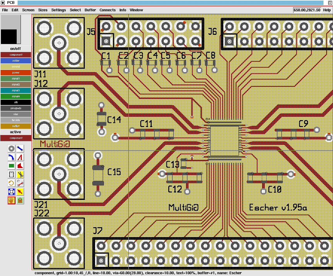
world technical: PCB version 3.0 printed circuit board layout tool

How to solve PCB switching noise with simple layout rules - Planet Analog

How to Design a PCB Layout - Circuit Basics

Schematic vs. Layout: PCB Geometry, Parasitics, and Signal Integrity

How to Distinguish the First, Second and Third Orders of HDI PCB - RAYPCB

Mastering the Art of PCB Design Basics | Sierra Circuits